
1958–1959 (experimental circuit and planar integration concept) / Americas
Integrated circuits bring components and connections onto semiconductor material
Kilby’s working circuit and Noyce’s planar integration concept offered different routes toward manufacturing electronic components and their connections together.
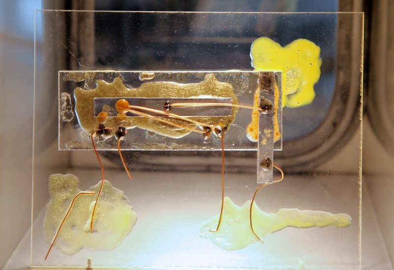
Image unavailable. The caption and source are still available.
The story
At Texas Instruments in 1958, Kilby demonstrated components formed on one piece of germanium and connected by fine wires. In 1959, Noyce at Fairchild used Hoerni’s planar process to conceive metal interconnections over an oxide layer and filed a patent. Working Fairchild monolithic circuits followed in 1960. Experiments, designs, patents and mass production were distinct stages involving many contributors.
Connections and context
Transistors supplied components; integration addressed the difficulty of connecting large numbers of separate devices. Miniaturization also depended on lithography, purified materials, packaging and reliability research.
Dates and precision
1958–1959 (experimental circuit and planar integration concept) Ongoing process
The dates describe a span of activity; the timeline uses its starting point.
Representative map location
Dallas and the US semiconductor research network
Dallas represents Texas Instruments’ work; Noyce and the Fairchild team worked in California.
Representative coordinates · 32.7767°, -96.797°
A marker identifies one representative place, such as a manuscript collection, laboratory or observing site. It does not mean the work happened only there, or assign a shared discovery to one country.
Bibliography
- Computer History Museum: The Integrated Circuit
- Computer History Museum: Practical Monolithic Integrated Circuit Concept Patented
- Jack S. Kilby: Nobel Lecture
References are listed as plain bibliography titles. They support particular facts or context; a reference does not certify every interpretation in a story.